
For chip processing
Share the part number, package photos, quantity, current marking or organization, and the required result. Samples or prior test data may help clarify feasibility.
From an individual DRAM IC processing step to a project connecting PCBs and memory modules, we work around the product and its intended use.
 Tynsen photo
Each service can be discussed on its own. Where several stages are connected, our teams can review the interfaces between them.
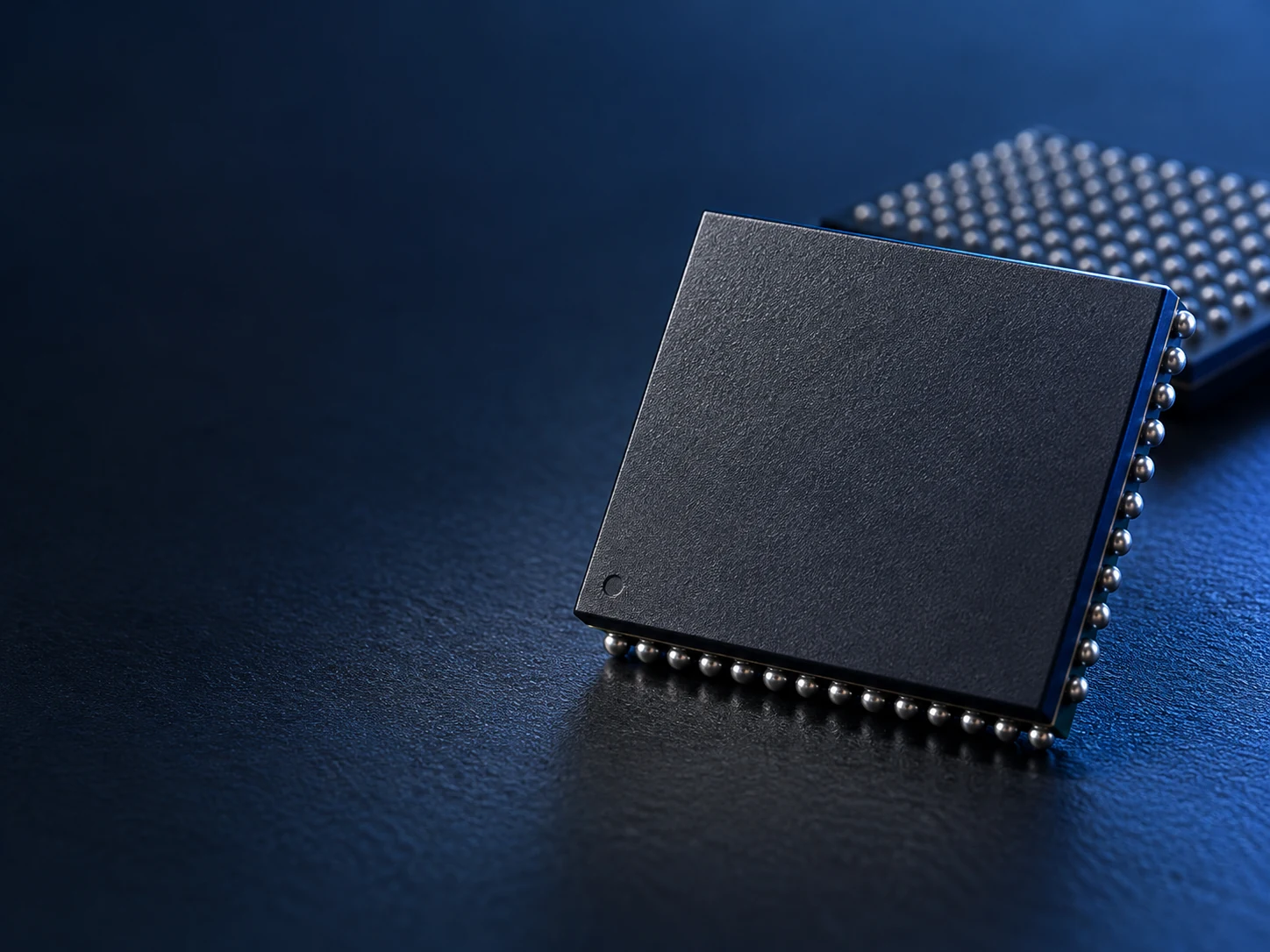 01 / COMPONENT
Reballing, surface grinding and laser remarking, configuration conversion, and IC testing.
Explore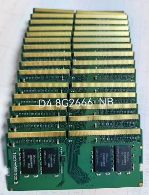 02 / CIRCUIT
PCB design, development, and manufacturing for memory products.
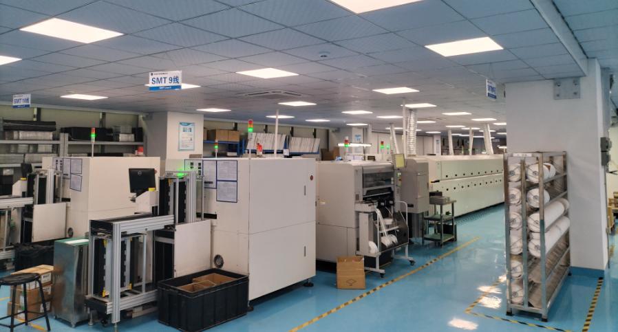
Explore03 / ASSEMBLYSMT assembly and related manufacturing for DDR3 and DDR4 memory modules.
Explore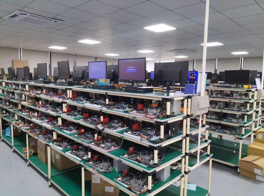 04 / SUPPORT
Memory module testing and repair, with the work scoped to the reported issue.
ExplorePart or module details, incoming condition, and the intended result give us a starting point. Any missing information can be clarified as the project progresses.
Share the part number, package photos, quantity, current marking or organization, and the required result. Samples or prior test data may help clarify feasibility.
Share target module requirements, board drawings if available, the DRAM parts, quantity, and any handling or test expectations.
Describe the observed issue, the affected products, and any previous results. These details guide the discussion of checks and corrective work.
Engineering, production, quality, and customer service support the stages relevant to the agreed project scope.
Review the device, incoming condition, and intended result
Agree on the process, inspection points, and acceptance criteria
Carry out the agreed processing or manufacturing
Complete the agreed checks and hand over the material and records
Before work begins, we can agree on processed material, samples, inspection points, test scope, marking information, and any records needed at handover.
We welcome a conversation about your memory project.