
Product target
Module family, capacity target, form factor, intended system, and any mechanical constraints.
We consider how the board fits the target memory module, DRAM components, and subsequent assembly. Projects can begin with existing drawings or with a set of product requirements.
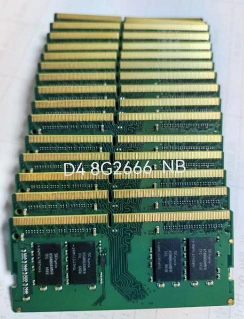 Tynsen photo
We provide memory PCB design, development, and manufacturing. Where PCB and SMT assembly belong to one project, we can review the requirements together from the outset.
Board drawings or design inputs
Target module and DRAM component information
Quantity and assembly requirements
Inspection and acceptance documentation
Board material, layer count, tolerances, and acceptance documentation are defined against the approved product requirements. We do not assume a single specification fits every memory module.
A memory PCB needs to fit both the electrical design intent and the downstream build. The earlier those interfaces are discussed, the easier it is to establish a coherent manufacturing scope.
Module family, capacity target, form factor, intended system, and any mechanical constraints.
Schematics, Gerber files, stackup, BOM, drawings, or a reference board can be reviewed where available.
DRAM part choice, component placement, panelization, inspection, and test needs are considered with the intended build.
Tynsen can discuss PCB work as a board-only project or as part of a module manufacturing program. Revision control, sample approval, inspection documents, and any assembly linkage are established in the project scope.
We welcome a conversation about your memory project.